2D MOFtronics
Dr. Renhao Dong
![Schematic illustration of MOFtronics.[14,16]](/529742/original-1678365605.jpg?t=eyJ3aWR0aCI6MzQxLCJmaWxlX2V4dGVuc2lvbiI6ImpwZyIsIm9ial9pZCI6NTI5NzQyfQ%3D%3D--486f46e0e8e6ca8fb83b83a3fb570c348d115f63 "Schematic illustration of MOFtronics.[14,16]")
![Schematic illustration of MOFtronics.[14,16]](/529742/original-1678365605.jpg?t=eyJ3aWR0aCI6MjQ2LCJvYmpfaWQiOjUyOTc0Mn0%3D--ef0d086bb135f2f66a5908b4493af424d3b6e236)
Schematic illustration of MOFtronics.[14,16]
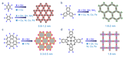
Two-dimensional (2D) π-conjugated metal-organic frameworks (2D c-MOFs) refer to layer-stacked MOFs linked by square-planar complexes with in-plane π-extended conjugation. They have similar structural features to graphite and other van der Waals layer-stacked materials, and in recent years have displayed much higher conductivities (up to 2500 S/cm) than conventional three-dimensional (3D) MOFs (<10-8 S/cm),[14] or demonstrated charge mobility of 220 cm2/Vs with band-like transport.[15] The enormous chemical and structural diversity of ligands and metal ions provides researchers with a playground filled with infinite creative possibilities, allowing design of 2D c-MOFs.[16] Although there are no commercial devices that yet incorporate 2D c-MOF materials, numerous proof-of-concept device demonstrations have appeared, such as transistors, photodetectors,[17] sensing, magnetics,[18,19] and energy storage[13,20,21] and conversion[22,23]. These advances are highly inspiring and demonstrate that 2D c-MOFs are an emergent class of layered electronic materials.
Research Area I. Chemistry of 2D conjugated MOFs
To date, around fifteen 2D c-MOFs have been reported based on planar polycyclic aromatic ligands (such as benzene, triphenylene, coronene, phthalocyanine and dibenzo[g,p]chrysene derivatives) with symmetrical functional groups (-OH, -NH2, -SH).[14,16] First of all, we aim to explore the influence of molecular design (type and geometry of ligand, metal) and material structure (redox-activity in linkage, layer stacking and arrangement) on the charge transport properties for 2D c-MOFs. Secondly, another essential question is how to optimize the reaction conditions to pursue high crystallinity.[24] Traditional approaches for controlling crystal growth generally involve varying solvent, concentration, reaction temperature, and time. Nevertheless, these strategies have failed in suppressing the anisotropic growth of a crystal because the in-plane metal-coordination bonds are too strong while the π-π stacking interaction is relatively weak. Thus, the crystal growth is usually dominated by the more reversible π-interaction to yield needle-like morphology with limited crystalline domains parallel to the intralayer direction, or even polycrystalline powders with tiny crystallites (up to hundreds of nanometers in size). Therefore, a rational ligand design will be the first step for establishing highly crystalline sample, thus achieving intrinsic electronic properties. On the other hand, we also explore a variety of synthetic methods to develop 2D c-MOFs, such as solvothermal synthesis, interface-assisted synthesis, on-surface synthesis and surfactant-assisted synthesis as well as CVD synthesis, which render 2D c-MOFs with various morphologies such as bulk crystals, ultra-thin nanosheets (<5 nm), and single-/few-layer films.

Research Area II. 2D c-MOFs for (Opto-)electronics and Spintronics
electronics.")
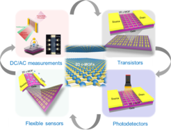
The high-conductivity or high-mobility 2D c-MOFs with tunable band structures exhibit promising potential as fascinating electroactive layers for opto-electronic devices. We are particularly interested in defining their intrinsic photo-/electron-transport properties via DC (like time-resolved terahertz spectroscopy) and AC measurements (like 2 probe, Hall effect and Van der Pauw).[15,17] As a consequence, we expect to establish a reliable structure-property relationship and achieve superior device performance for transistors, photodetectors and sensors.
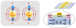
Spintronics, also known as spin transport electronics, has been intensely researched for the next generation of quantum computing and data storage, because spintronics could offer an exciting prospect of combining the semiconductor-based information operation (logic) and magnetic based data storage (memory) into the same device. Historically, spin-related phenomena have been widely studied in inorganic semiconductors; however, the entirely inorganic composition prevents a facile tunability of magnetic and conductive properties due to the lack of both ligand functionalization and structural diversity. In this respect, (semi-)conductive 2D c-MOF hold promise because the magnetic behavior can be tailored at the molecular scale through tuning their building blocks, metal centers (spin carriers) and even filling functional guest molecules or introducing radicals into the porous. For this purpose, we aim at the design and synthesis of 2D c-MOF magnets for spintronics.

Research Area III. 2D c-MOFs for Electrochemical Energy Storage/Conversion
Conductive 2D c-MOFs incorporating redox active units have emerged as a novel class of multifunctional electrode materials for electrochemical energy storage. Metal-ion batteries and supercapacitors represent two major energy storage devices. Benefiting from the intrinsically conductive and porous properties, 2D c-MOFs have shown excellent performance in metal-ion batteries[21] and supercapacitors,[20] which could function as the power sources for the above mentioned MOFtronics.
![Schematic illustration of 2D c-MOFs for electrochemical energy storage. (a) Li-ion battery.[21] (b) Flexible microsupercapacitor.[20]](/529871/original-1621423777.jpg?t=eyJ3aWR0aCI6MzQxLCJmaWxlX2V4dGVuc2lvbiI6ImpwZyIsIm9ial9pZCI6NTI5ODcxfQ%3D%3D--31a7428251c019d8fc5b4ee7c1ea31720f2284bd "Schematic illustration of 2D c-MOFs for electrochemical energy storage. (a) Li-ion battery.[21] (b) Flexible microsupercapacitor.[20]")
![Schematic illustration of 2D c-MOFs for electrochemical energy storage. (a) Li-ion battery.[21] (b) Flexible microsupercapacitor.[20]](/529871/original-1621423777.jpg?t=eyJ3aWR0aCI6MjQ2LCJvYmpfaWQiOjUyOTg3MX0%3D--73be3790560fec4b264afefcc506e676915c9ad7)
The exploration of effective electrocatalysts has advanced the development of electrochemical energy storage and conversion technologies, such as fuel cells, water splitting, and metal–air batteries. 2D c-MOFs are highly attractive catalytic systems due to the uniquely combining homogenous and heterogeneous features: 1) the incorporation of well-defined and highly active sites into a defined and stable scaffold ensures excellent catalytic activity and selectivity; 2) the porous metrics allow for sufficient and controllable mass transfer to and from the embedded active sites; 3) the molecularly defined catalytic environment around the active site allows for tuning the catalytic reaction by modifying the scaffold and facilitates deriving fundamental understanding of catalytic mechanism. To achieve high catalytic performance, our research focus on the design and synthesis of novel 2D c-MOFs with well-defined active sites and porous structures for mass transfer.
![Schematic illustration of 2D c-MOFs for electrochemical energy conversion, including HER,[2,25] ORR22 and CO2RR.[23]](/529932/original-1673433947.jpg?t=eyJ3aWR0aCI6ODQ4LCJmaWxlX2V4dGVuc2lvbiI6ImpwZyIsIm9ial9pZCI6NTI5OTMyfQ%3D%3D--e00875160e9b7d0a60b2fa729d0571cd2346dc98 "Schematic illustration of 2D c-MOFs for electrochemical energy conversion, including HER,[2,25] ORR22 and CO2RR.[23]")
![Schematic illustration of 2D c-MOFs for electrochemical energy conversion, including HER,[2,25] ORR22 and CO2RR.[23]](/529932/original-1673433947.jpg?t=eyJ3aWR0aCI6MjQ2LCJvYmpfaWQiOjUyOTkzMn0%3D--297d657355f5ddbf069a358f6955d1d622032f75)