Low Temperature Scanning Probe Microscopy

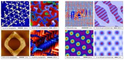
Local probe instruments like the scanning tunneling microscope (STM) or the atomic force microscope (AFM) are surface characterization methods with ultimate space resolution. Working in a low-temperature setup they unfold a great arsenal of analysis methods by enabling high-resolution local spectroscopy under ultra-stable conditions. The pictures on the right show some examples of STM real space imaging of sample areas ranging from a few nanometers to several 100 nm scales.
NISE Lab
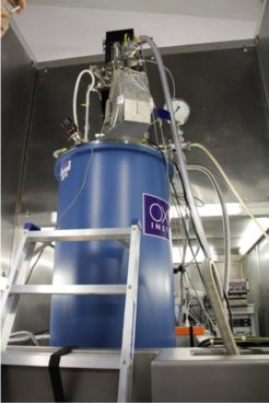
Our laboratory stands on exceptionally low-noise concrete foundation, the microscope systems are additionally separated from the surrounding floor and housed in acoustic shields to minimize environmental influences. The institutes liquid helium network is well connected and recovers evaporated helium to send it back to a large liquefier to ensure cryogenic supply. Further, the institutes portable vacuum suitcases enable us to measure samples grown by our MBE experts next door. The two currently running systems (3He-STM and MFM) will soon be extended to four low temperature scanning probe microscopes. In our 3He-STM system we achieved all of our recent results (see publication list for reference). It reaches a temperature of 500mK and is equipped with a 6-1-1 Tesla superconducting vector magnet.

We readily conduct
- atomic-scale imaging,
- local density of states spectroscopy with sub-meV resolution,
- >24h full spectroscopy grids,
- quasiparticle interference derived momentum-space imaging,
- in-situ atom deposition,
- atomic manipulation,
- tip functionalization for superconducting or magnetic tips facilitating spin contrast maps and Josephson spectroscopy.
Our low-temperature performance will soon reach new horizons with the already ordered UNISOKU USM 1600 ultra-low temperature SPM system. The dilution fridge cryostat allows continuous measurement below 50mK, it is equipped with additional RF lines for high frequency experiments, a 9-2-2T vector magnet and ready for qplus© AFM. The ultra-low temperature makes it the ideal tool to study superconducting phenomena including triplet superconductivity and magnet-superconductor quantum interfaces via e.g. Josephson STM.
We are currently setting up a home-built LTSTM system with 1.5K base temperature and a unique 12T external magnetic field along any sample direction. It will be our most flexible system for custom-built low- temperature SPM experiments. There is an additional variable temperature STM connected to its preparation chamber allowing for quick checks of sample morphologies in order to enhance productivity and growth optimization.
Working in the LTSPM lab
Scanning probe microscopy is an extremely powerful surface characterization method, however, it is technically challenging. Working with these systems will grant you expertise with ultra-high vacuum and ultra-low temperature, deep technical understanding on femto-scale current detection including means to reduce noise sources to a minimum. It requires the readiness to yield a wrench and to manipulate samples in vacuum with a steady hand on the wobblestick. On the scientific side, it proves very rewarding, provided a little patience, due to the variety of information one might extract from a material surface with unique real space resolution.
Research prospects
Every microscope system is directly connected to a preparation chamber where we can do Ar sputtering, annealing and even some basic MBE. However, the big advantage of working at Max Planck in Halle is the opportunity to have immediate contact to many scientists that focus on synthesizing new atomically engineered materials with potential application in spintronics, large and efficient data storage technology or quantum computing. In order to achieve that, we interface magnetism and superconductivity at the quantum level looking for unconventional superconductors like triplet and topological superconductors or high-TC superconductors. We are investigating epitaxial thin films, 2D materials, heterostructures, Van-der-Waals layered crystals, cleaved single crystals, MBE grown nano-islands and STM tip assembled nanostructures.

