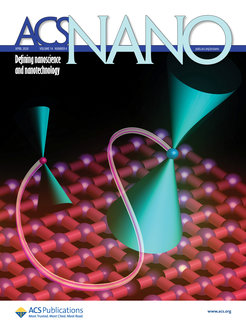
Growth of Weyl semimetal NbP and TaP thin films - published in ACS Nano
We are pleased to announce that our paper on "Realization of Epitaxial NbP and TaP Weyl Semimetal Thin Films" has been published in ACS Nano and is now accessible online.
Abstract

Weyl semimetals (WSMs) exhibit an electronic structure governed by linear band dispersions and degenerate (Weyl) points that lead to exotic physical phenomena. While WSMs were established in bulk monopnictide compounds several years ago, the growth of thin films remains a challenge. Here, we report the bottom-up synthesis of single-crystalline NbP and TaP thin films, 9 to 70 nm thick, by means of molecular beam epitaxy. The as-grown epitaxial films feature a phosphorus-rich stoichiometry, a tensile-strained unit cell, and a homogeneous surface termination, unlike their bulk crystal counterparts. These properties result in an electronic structure governed by topological surface states as directly observed using in situ momentum photoemission microscopy, along with a Fermi-level shift of −0.2 eV with respect to the intrinsic chemical potential. Although the Fermi energy of the as-grown samples is still far from the Weyl points, carrier mobilities close to 103 cm2/(V s) have been measured at room temperature in patterned Hall-bar devices. The ability to grow thin films of Weyl semimetals that can be tailored by doping or strain, is an important step toward the fabrication of functional WSM-based devices and heterostructures.


